Detailed Introduction of the Chip Design Process
Table Of Content

Saligane says such research is critical and will not be impacted by a parallel approach to encourage and enable more participation in the design process. Synopsys is a leading provider of electronic design automation solutions and services. In order to validate the silicon from the manufacturability issues, the concept in the Chip Designing is Design for Test(DFT).
AI Chips vs. Traditional CPUs and GPUs
Semidynamics Provides All-In-One AI IP to Facilitate AI Chip Design - News - All About Circuits
Semidynamics Provides All-In-One AI IP to Facilitate AI Chip Design - News.
Posted: Thu, 11 Apr 2024 07:00:00 GMT [source]
They have very good footprint in automotive and aerospace vertical. So just to clarify, we have the same strategy from ‘18, and that's doing working as well. It's primarily organic with very synergistic computational software, mostly tuck-in acquisitions. Before I provide our updated outlook, I'd like to share some assumptions that are embedded in our outlook. Given the recent launch of our new hardware systems, we expect the shape of hardware revenue in 2024 to weigh more toward the second half, as our team works to build inventory of the new system. Our updated outlook does not include the impact of our [pending] (ph) BETA CAE acquisition and it contains the usual assumption that export control regulations that exist today remain substantially similar for the remainder of the year.

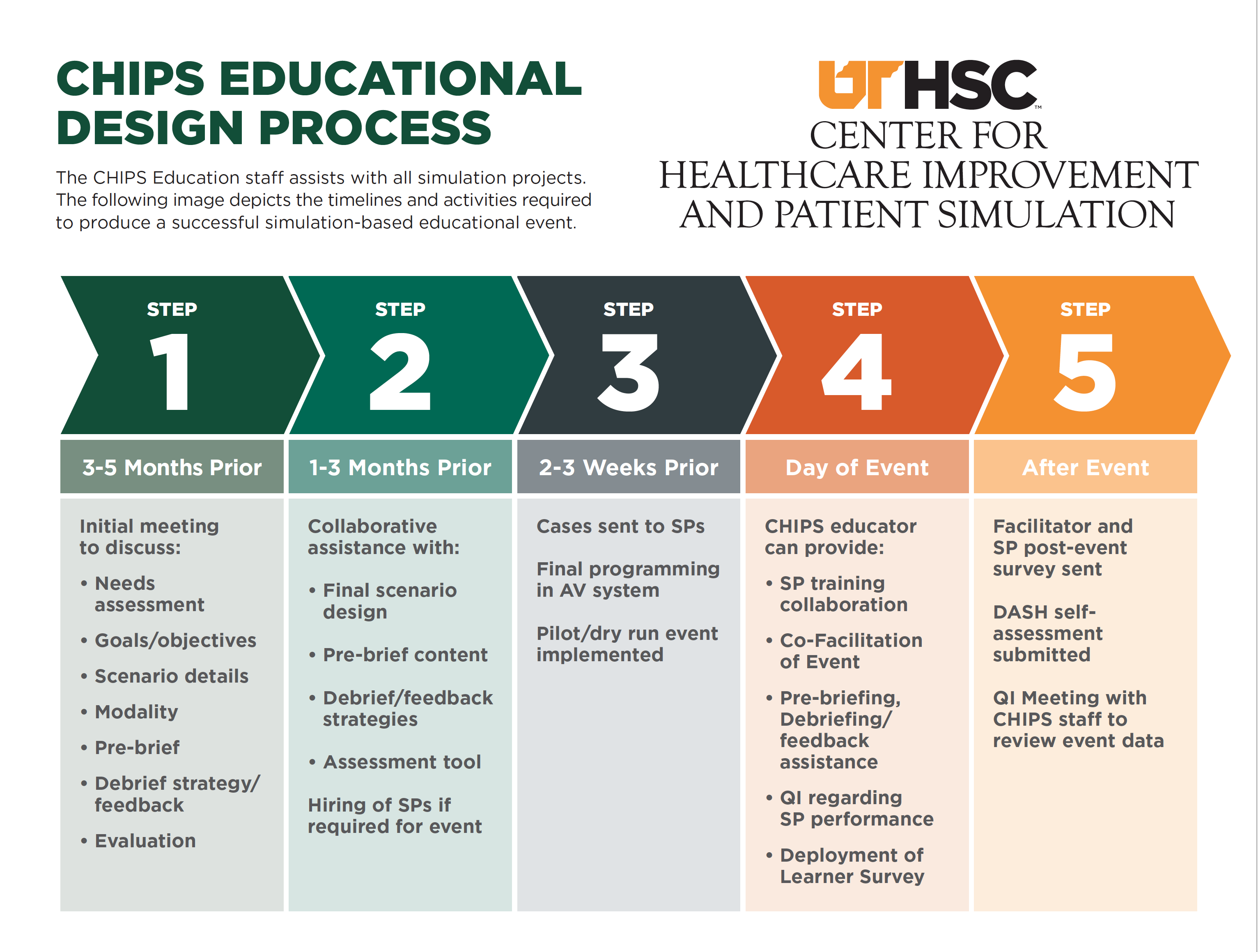
Step 1: Product definition and specification
The final step is the fabrication of the physical layout design. While designing system on the tools, all the libraries and layer information is provided by the foundry which is going to fabricate the chip. After the system is designed and verified, a .GDS file is sent to foundry for fabrication. The figure below shows physical layout of the half adder, here one can observe that as the modules are linked together, the process becomes tougher. The first and most important step of the chip design process is defining and creating the specification of the system. The main purpose of the system is to get multiplied 2 4-bit inputs.
Gravit Designer
You know, and yes, we talked about our new partnership on Total Compute. Also, I think this quarter we talked about our partnership with HARMAN Automotive. Because what is interesting to see, which of course you know this already, but Arm continues to do well in mobile, but also now in kind of HPC server and automotive end markets. The time -- it's good to accelerate the -- because these AI chips are getting bigger and bigger, right? So the demand for emulation is getting bigger and bigger, and I can give you more stats later.
Affinity Designer
ASICs are typically used in high-performance applications where specific processing requirements need to be met, such as in networking, telecommunications, and consumer electronics. ASICs are designed and manufactured for a specific customer or application and can include digital, analog, and mixed-signal components on a single chip. The University of Michigan is part of a growing movement to make integrated circuits (IC) or chip design more accessible by providing open-source process design kits (PDKs), EDA tools, and building blocks.
US guru says China’s supercomputer power may exceed all countries
Nvidia Trains LLM on Chip Design - EE Times
Nvidia Trains LLM on Chip Design.
Posted: Mon, 30 Oct 2023 07:00:00 GMT [source]
For EDA, where chip design-related data is largely proprietary, generative AI holds potential for supporting more customized platforms or, perhaps, to enhance internal processes for greater productivity. AI can come up with the right set of parameters that delivers the highest ROI in a big solution space in the fastest possible time. In other words, better (and faster) quality of results than otherwise possible.
Indeed, some 65 percent of students pursuing advanced degrees in electrical engineering and computer science in the United States are foreign nationals. However, these students often encounter labor restrictions that curtail their employment opportunities in the United States upon graduation. As a result, companies frequently transfer these skilled workers to their overseas subsidiaries, enabling them to continue contributing to U.S. enterprises.
Engineers would add the sketches to their microchip designs in the techie equivalent of signing their artwork. They'd etch them on chips that may end up in your cellphone, laptop or calculator. They spent hours crafting them, even though they were frowned upon by those in the C Suite. All painstakingly selected and etched onto a microchip that measures about an inch square. Each microscopic silicon doodle was the handiwork of engineers at Qualcomm Incorporated, a San Diego-based company that creates wireless technology-related products and services. The engineers slipped the drawings into Qualcomm's Q1650 data decoder with care not to disturb any of the chip's functions.
Define the main functional units of the system to help identify the interconnection requirements between the units, as well as the physical and electrical specifications of each unit. ASIC can be found in almost any electronic device, and its uses range from the custom rendering of images to sound conversion. Since ASICs are custom-made, they can only be used by the company that designed them, so they are considered proprietary technologies. Launched in 2018 with $32 million, it is currently funded through a government-industry consortium and includes 21 faculty members and 130 graduate students from 11 universities.
And I mentioned Qualcomm last week talked about pretty impressive results because verification, as you know is an exponential problem, because as the chips get bigger, the verification task gets exponentially bigger. Okay, Anirudh so [piggyback] (ph) to your conference last week, particularly the Gen AI track, it was interesting of course to hear the adoption presentations by Renesas, Intel and so forth. But what seemed to be taking place is a heavy focus on Cerebrus which makes sense, it is the one longest end-market. So perhaps you could talk about how you are thinking about the adoption curve for the other brands aside from Cerebrus?
Ion implantation is an important doping technology in the chip manufacturing process, and it is also an important means of controlling the threshold voltage of the MOSFET. The part covered by the photoresist, the ion beam cannot penetrate the photoresist and is blocked; the part not covered, the ion beam will be implanted into the substrate to achieve doping, and the doping depth depends on the ion beam energy. Finally, after the ion implantation is completed, the photoresist must be thoroughly removed before proceeding to the next step. The logic design gives a simplified logic implementation, while the circuit design further expresses the logic in the form of a netlist. The netlist is usually composed of gates, transistors, and various interconnections.
According to the circuit structure engraved by the photoetching machine, micro-engraving is carried out on the silicon wafer to engrave grooves or contact holes. The first step is to saw the monocrystalline silicon ingot into a disc horizontally, then polish and crystallize it to obtain a mirror-like wafer. At this time, pure silicon will go through a high-temperature furnace filled with oxygen to form a very thin layer of silicon dioxide on the surface as the gate oxide layer of the transistor.


Comments
Post a Comment